 |
 |
|
 |
| |
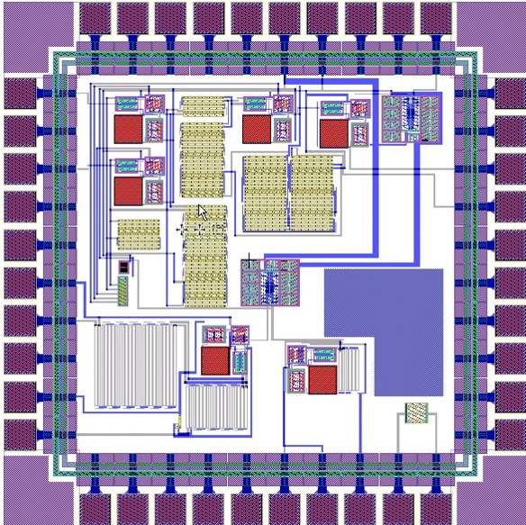
A
set of multi-dimension MOS transistors for device characterization
The
aim of the design is to provide test structures for extracting
the threshold voltage and the effective channel length and
width of the MOS transistor. The characterization is to be
accomplished through the measurement of the drain current
somewhere between weak and moderate inversion, since it is
based on the change of the slope of the device I-V characteristic
from weak to moderate inversion.
Fabrication
Technology: 1.5; 0.5; 0.35 and 0.18 um
[Report]
Designer:
Márcio Bender
Date:
2003
|

|
|
| |
NMOS
and PMOS Transistor Arrays for Current Mismatch Measurement
Fabrication
Technology: 1.5; 0.5 and 0.35 um
[Report]
Designer:
Hamilton Klimach
Date:
2003
|
 |
|
| |
Body-Bias
Compensation Technique for Subthresold CMOS Static Logic Gates
Fabrication
Technology: 1.5 and 0.35 um
[Report]
Designer:
Luiz Alberto Pasini Melek
Date:
2003
|
 |
|
| |
An
Ultra-Low-Power Self-Biased Current Source
Fabrication
Technology: 1.5; 0.35 and 0.18 um
[Report]
Designer:
Edgar Mauricio Camacho Galeano
Date:
2003
|
 |
|
| |
A
gm-c Bump Equalizer for Low-Voltage Low-Power Applications
Fabrication
Technology: 0.35 um
[Report]
Designer:
Renato Galembeck and Marcelo Luiz Poleto
Date:
2004
|
 |
|
| |
An
instrumentation amplifier applied to a high sensitivity Piezoresistive
silicon pressure transducer
Fabrication
Technology: 0.35 um
[Report]
Designer:
Márcio Bender and Gustavo Giusti
Date:
2004
|
 |
|
| |
A
low-power 8 bits successive Approximation ADC using Binary
weighted capacitors
Fabrication
Technology: 0.35 um
[Report]
Designer:
Edgar Mauricio Camacho Galeano
Date:
2004
|
 |
|
| |
A
1,8 - 5,5 GHz five-port front-end
Fabrication
Technology: AsGa 0.20 um
Designer:
Fernando Rangel de Sousa
Date:
2004
|
 |
|
 |
|
|
 |