An Ultra-Low-Power Self-Biased Current Source
Summary
To: MOSIS
Submitted by: Edgar
Mauricio Camacho Galeano, maoedgar@eel.ufsc.br
Professor: Márcio Cherem Schneider,
marcio@eel.ufsc.br
Affiliation: Integrated
Circuits Laboratory-Department of Electrical Engineering-Federal University of
Santa Catarina. (www.eel.ufsc.br/lci)
Project Title:
Design of an Ultra-Low-Power Current Source
Fabrication Technology: AMI-1.5mm, TSMC 0.35, TSMC 0.18
Objective: To design a current source
for technology-independent inversion
level biasing.
Challenges: 400pA-5nA (1nW-40nW) current sources (self-biased)
sub-1V.
Expected Publications: Master degree
work; publish our results in international conferences.
Simulation support: Smash circuit simulator, L-edit Tanner.
Chip size: 1.5mmx1.5mm
(Tiny Chip)
Test: Measurement of DC characteristics, PSR and
start-up time.
Equipment: TDS2014
tektronix, HP4145, HP3245A, HP E3610A, HP 3588A.
Packaging: DIP-
40.
Overview
CMOS analog design based on the inversion level
technique has been shown to be a robust alternative for high performance in
very-low-power [1] and low-voltage circuits [2]. This technique uses the
current as the main design variable. Thus, analog circuits based on such a
design technique require a self-biased current source (SBCS) to operate at the nominal inversion level. Moreover, the
generation of on-chip current references avoids the need for an extra pad to
communicate with the external environment.
Several SBCS circuits are found in the
literature [3] - [6], but, none of them are suitable for very low currents
required for ultra-low-power applications, as in [1]. Our SBCS is based on the circuits proposed in [3], [4], [5], and [6],
which have the same current dependence on temperature. Despite the simplicity
of the circuit proposed in [3], it uses a resistor that for small currents
(pA-nA) consumes a very large silicon area. To avoid the need for a resistor,
the authors of [5] use a MOSFET working in the triode region to replace the
resistor. Even though simple, the SBCS of [5] is not suitable for low voltage
operation, as pointed out in [6]. Another implementation of an SBCS is
presented in [4] but the large current gains and operation in strong inversion
of some of its transistors degrade its power efficiency. Reference [6] presents
another proposal of an SBCS, a less simple structure than the previously
mentioned ones. This circuit uses a self-cascode MOSFET (SCM) in strong
inversion and a PTAT voltage reference generated by means of a current ratio.
Although appropriate for low voltage operation, the power efficiency of the
current source in [6] is not high due to the use of slightly more complex
structures and operation in strong inversion of some transistors.
Project Description
This project proposes a power efficient self-biased current source dedicated to technology-independent inversion level biasing, which is suitable for low-voltage and very low power applications. Our SBCS circuit uses MOSFET’s only and can operate down to 1V supply voltage and exhibits low sensitivity to temperature and to supply voltage from simulation results. A 400pA (TSMC 0.35um) and 650pA (TSMC 0.18) current source is designed and was simulated using SMASH with BSIM3V3 model.
Simulations show that for TSMC 0.35um and TSMC 0.18um CMOS technologies, it circuit can operate from a supply power of 0.8V and 0.65V, respectively. The circuit will be tested in our laboratory, where all required equipment is available. The total silicon area needed including pads and test circuit is estimated at 1.5mmx1.5mm.
To characterize our chip, we will use an HP 4145B semiconductor parameter analyzer, an HP 3588A spectrum analyzer and a Tektronix TDS2014 digital oscilloscope.
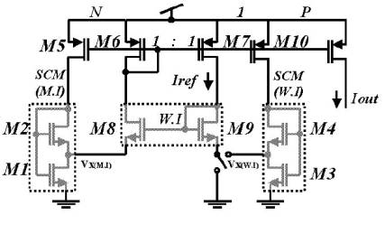
Figure
1. Self-biased current source circuit.
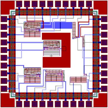
LAYOUT
References
[1] B.Linares-Barranco and T.
Serrano-Gotarredona, “On the design and characterization of femtoampere
current-mode circuits” IEEE J. Solid-State Circuits, vol. 38, pp.
1353-1363, August 2003.
[2] S. Yan and E. Sánchez-Sinencio,”Low voltage analog circuit
design techniques: A tutorial” IEICE Trans. Fundamentals, vol. E00-A, No.2, pp. 1-17, February 2000.
[3] E. Vittoz and J. Fellrath,
“CMOS analog circuits based on weak inversion operation,” IEEE J. Solid-State
Circuits, vol. SC-12, pp. 224-231, June 1977.
[4] E.A
Vittoz and C.C Enz, “CMOS low-power analog circuit design”, proceeding of the
International Symposium of Circuits and Systems (ISCAS’96), chapter 1.2 of
Tutorials.
[5] H. J.
Oguey and D. Aebischer, “CMOS current reference without resistance,” IEEE J.
Solid-state Circuits, vol. SC-32, pp. 1132-1135, July 1997.
[6] F.
Serra-Graells and J. L. Huertas, "Sub –1-V CMOS proportional-to-absolute
temperature references", IEEE J. Solid-State Circuits, vol. 38, no. 1, pp.
84-88, Januery 2003