Universidade
Federal de Santa Catarina
Departamento de
Engenharia Elétrica
Laboratório de
Circuitos Integrados
Mosis 68589 - Body-Bias
Compensation Technique for Subthreshold CMOS Static Logic Gates
Designer: Luiz
Alberto Pasini Melek
Professor: Carlos
Galup-Montoro
Technology: TSMC
0.35
Design sent: 09/23/2003
Design received: 12/05/2004
(wrong project) 01/07/2004 (right project)
Report sent to MOSIS:
02/24/2004
Mosis 68680 - Body-Bias
Compensation
Technique for Subthreshold CMOS Static Logic Gates
UNIVERSIDADE
FEDRAL DE SANTA CATARINA - UFSC
LABORATÓRIO
DE CIRCUITOS INTEGRADOS - LCI
Mosis
69011 - A set of multi-sized MOS transistors for device
characterization
1.Description
of Project
Summary
To: MOSIS
Submitted
by: Márcio Bender MachadoLuiz
Alberto Pasini Melek - marciobmpasini@eel.ufsc.br
Professor: Márcio Cherem Schneider, marcio@eel.ufsc.br
Affiliation: Integrated Circuits Laboratory, Department of
Electrical Engineering, Federal University of Santa Catarina.
(www.eel.ufsc.br/lci)
Project
Title: Body-Bias
Compensation Technique for Subthreshold CMOS Static Logic GatesA set of multi sized MOS
transistors for device characterization
Fabrication
Technology: AMI 1.5 and TSMC TSMC 00.335 um
Objective: To extract the threshold voltage and effective
channel length and width in single-crystal bulk MOSFETsMeasure
DC transfer and transient response of body-biased digital
gates
Challenges: To provide a simple and objective methodology for
the extraction of threshold voltage and effective channel length and width. The
methodology of extraction is fully consistent with the Advanced Compact MOSFET
(ACM) model and requires moderate-resolution equipment only.Verify
and analyze the subthreshold operation of digital
circuits body-biased by three different circuits
Expected Publications: Papers in scientific journals, and international
conferences, technical reports and a
master degree dissertation.
Simulation support: Smash circuit simulator,
Tanner tools.
Chip size: 1.51.5mm
x 1.51.5mm
Test: Measurement of DC characteristics and
transient response.
Equipment: HP4145 and
oscilloscope.
Packaging: DIP- 40.
Project
Description
The use of portable equipment such as cellular
phones, hand-held devices, laptops, and hearing-aid devices is increasing
tremendously. Battery-operated equipment should be small and light. Therefore,
if performance is not of primary importance, the power consumption should be
kept to a minimum [1], [2]. Ultra-low power circuits are still in their
infancy. One of them is a digital FIR filter [3] that can be used for
biomedical signal detection, identification tags and smart cards. It is an
8-tap, 8-bit filter that dissipates only 4.75mW, at 1V supply and 500kHz clock frequency. In [4],
a voice controlled digital video decoder specific for wristwatch applications
operating at 1V, 1MHz dissipates only 60mW. To achieve
the requirements of (ultra)-low power dissipation in the range of a few
microwatts, although still working at several megahertz, as in these
applications, static logic gates operating in subthreshold are strong
candidates [1].
The
subthreshold current of a MOSFET is very sensitive to temperature and process
parameters, and so is its performance. As a consequence, the rise and fall
times of an inverter will differ by an order of magnitude or even more. The
result is a waste of energy due to the higher current since the switching
frequency is mostly determined by the higher of the rise and the fall times.
So, compensation techniques must be applied to compensate the drive currents
and avoid wasting too much energy.
In Fig. 1, we show three circuits that can be used
to compensate for process variations by providing an appropriate body-bias
voltage, VW. In any of the three bias circuits, the voltage VW
stabilizes at a value such that the current of the PMOS and NMOS devices are
the same. In these circuits, two source-to-bulk diodes are forward-biased;
thus, the compensation techniques should be limited to sub-1V power supplies.
The circuit in Fig. 1(a), which equalizes the “off” currents of the
complementary devices, has been proposed in [5] and has been a great source of
inspiration to our work. The circuit in Fig. 1(b) provides an equalization of
the driving currents while that in Fig. 1(c) equalizes the currents for an
input equal to the gate threshold voltage.
(a) (b) (c)


Fig 1:
Bias circuits
Since the digital circuits are operating in
subthreshold regime, the lower the threshold voltage, the lower the power
consumption, because supply voltage can be reduced. So, future technologies that
have lower threshold voltages tend to dissipate less power, but still work at
the same frequency. For this reason, we chose the TSMC 0.35μm technology
that has low threshold voltages compared to other technologies available from
the MEP research.
Estimated
Structures and Chip Size
To fully validate the proposal, some circuits such
as isolated NMOS and PMOS transistors, an inverter, a ring-oscillator, a latch,
and a binary counter modulo 10, working as test elements are being designed. The
design is being carried out to have the flexibility to allow compensation from
any of the three bias circuits shown in Fig1. The project is being designed
with the MOSIS Scalable CMOS (SCMOS) Design Rules and will be submitted to
TSMC0.35μm and AMIS1.5μm fabrication, in order to compare the results
in both technologies. It will occupy not more than 1.5mmx1.5mm in
TSMC0.35μm and 2.2mmx2.2mm in AMIS1.5μm die areas, including the
pads, since the test elements are small because minimum dimensions transistors
are being used. A conventional 40-pin ceramic package will be used for both
technologies.
Simulation
Plans
Simulations of the proposal have been carried using
the Smash circuit simulator available from Dolphin Integration with
AMS0.8μm, AMS0.35μm and TSMC0.35μm technologies. BSIM3v3
transistor model has been used.
The operation of CMOS static logic gates has been
analyzed by means of simulation. The influence of the technological parameters deviations
on the operation of the gates has been detected and three bias circuits have
been proposed to compensate for these deviations.
Test and
Characterization Plans
To test and
characterize the fabricated circuit several pieces of equipment are available
in our laboratory:
§TDS 220 digital real-time oscilloscope ( 2-channel,
100MHz, 1GS/s ) from Tektronix
§TDS2014 digital storage oscilloscope (4-channel,
100MHz, 1GS/s) from Tektronix
§HP 4145B Semiconductor Parameter Analyzer
§HP 3245A Universal Source
§HP E3610A/E3620A/3630A DC power supplies
§HP 3314A function generator.
We plan to
evaluate the performance of the test elements in the following ways. First, the
subthreshold operation of the transistors will be measured and technological parameters
will be extracted. Then transient response and maximum operating frequency of
the test elements will be determined and the correct bias circuit operation
will be verified. Third, total power dissipation will be measured and, if
possible, dynamic, static and short-circuit power dissipations will be analyzed
separately, to validate the proposed technique for ultra-low power circuits. To
finish, maximum and minimum operating supply voltages will be determined,
according to requested operating frequency.
References
[1] H. Soeleman, K. Roy, “Ultra-Low Power Digital
Subthreshold Logic Circuits”, International Symposium on Low Power
Electronics and Design, 1999, pp.94-96.
[2] H.
Soeleman, K. Roy, B. Paul, “Sub-Domino Logic: Ultra-Low Power Dynamic Sub-Threshold
Digital Logic”, IEEE International Conference on VLSI and Design, 2001,
pp211-214.
[3]
Amirtharajah, R., Chandrakasan, A., “Self-Powered Signal Processing Using
Vibration-Based Power Generation”, IEEE J. Solid-State Circuits, vol. 33, No.
5, May
1998.
[4] Bolcloni, L.,
Borgatti, M., Felici, M., Rambaldi, R., Guerrieri, R., “A low-power,
voice-controlled, H.263 video decoder for portable applications”, IEEE Journal
of Solid-State Circuits, vol. 33, no. 11, November 1998.
[5] A.
Bryant, J. Brown, P. Cottrell, M. Ketchen, J. Ellis-Monaghan, E. Nowak,
“Low-Power CMOS at Vdd=4kT/q”, Device Research Conference 2001.
Note
1.A Master
Degree dissertation based on the proposed bias circuits in Fig.1 is being
carried out. The fabricated circuit will allow experimental results and will
further validate the proposal, to be included in the dissertation.
1.A paper
based on the proposed bias circuits is being written and will be submitted to
ISCASS2004 and other seminars to be published in due course.
Overview
The
threshold voltage and the effective channel length and width of the MOS
transistor are fundamental parameters in CMOS technology for circuit design,
performance modeling and process control. There are numerous methodologies for
extracting the threshold voltage in the literature [1], each of them giving a
different interpretation or definition of the parameter. Since the methods
based on capacitance characteristics demand greater complexity in equipment,
most of the available procedures are based on the measurement of static drain
current characteristics. In general, these approaches exploit an asymptotic
behavior of the device, chiefly in strong inversion [1,2] but alternatively in
weak inversion [1], because the threshold voltage definition thus adopted is
attached to the device modeling in one of these particular regimes. Biasing the
transistor in the linear region is usually preferred in order to minimize short
channel effects [1,2]; nevertheless, some methods use the device
characteristics under saturation [1]. The enormous diversity of approaches
result in significant deviations between extracted values of the threshold
voltage from different methods, each of them of undetermined accuracy, and
prove that the estimation of such a parameter still remains an unsolved
problem.
A similar
picture may be outlined for the extraction of effective channel length. A great
number of methodologies exist [3-5], many of which associated with the series
resistance extraction since the voltage drops across the extrinsic drain and
source resistances are not negligible in the operating regime adopted for
measurements [3-5]. Most of the channel length extraction procedures require a
previous determination of the threshold voltage or take into account the
dependence of this parameter on channel length [4]. Such dependence affects the
accuracy of the methods.
Project
Description
The aim
of the design herein described is to provide test structures for extracting the
threshold voltage and the effective channel length and width of the MOS
transistor. The characterization is to be accomplished through the measurement
of the drain current somewhere between weak and moderate inversion, since it is
based on the change of the slope of the I-V characteristic of the device from
weak to moderate inversion. In such a region of operation the influence of
series resistance and the degradation of the transconductance factor due to
transversal field may be neglected. Therefore, the quadratic behavior of the
drain current characteristics, usually exploited in conventional methodologies,
is not to be applied.
We shall
follow two procedures, one with the transistor biased in the linear region and
the other with the device operating in saturation, though subjected to low
drain-to-source voltage to avoid small dimension effects to become important.
Both procedures are founded on the ACM (Advanced Compact MOSFET) model, which
furnishes simple expressions for the terminal voltages and gate and source
transconductances in terms of the forward and reverse saturation components of
drain current. Each expression is valid in all regimes of operation. The
interpretations of threshold voltage and effective channel dimensions are
consistent with the model.
The test
structures consist of a set of wide channel transistors with various channel
lengths to determine the effective channel length and a set of transistors with
intermediate channel length and various channel widths to determine the
effective channel width. Each transistor is composed of the parallel
association of unit devices to reduce the noise level compared to the signal
and average the measurements over a large area. A remarkable property of the
approach employed to extract the effective channel length and effective width
is the insensitivity to threshold values. Therefore, even small geometry
devices can be employed to extract the effective channel width and length.
1.Implemented Circuits
The circuit was implemented with two groups of
transistors: Group1, which is employed to determine the effective channel
length and VT, while group 2 is used to determine the effective width and VT. Both
groups of transistors are split into N and P-channel devices of seven
dimension, for the P channel as for N channel . The sizes of the devices are
·Set
1 or L
L1=Lmin
L2=1.5 Lmin
L3= 2 Lmin
L4= 2.5 Lmin
L5= 3 Lmin
L6= 4 Lmin
L7= 10 Lmin
Obs.: *
W=100 * L for all transistors.
·Set
2 or W
W1=Wmin
W2=1.5 Wmin
W3= 2 Wmin
W4= 2.5 Wmin
W5= 3 Wmin
W6= 4 Wmin
W7= 10 Wmin
Obs.: * L=3 * Lmin for all transistors.
* Each transistor is composed of the parallel
association of M devices, with M = 150
* (Wmin/W).
* M =
37.5 is approximated by 38.
All gates and sources of transistor P channels were
wired together. The same procedure was applied to the N-channel transistors, as
can be seen in Figure 1. Externally, the drain of each transistor, the gate of
transistors P (GP), the gate of transistors N (GN), the source of transistor P
(SP), and the source of transistors N (SN) were available. Besides these,
another four pads for the guard ring were used.
Obs.: The pads don´t have protection.
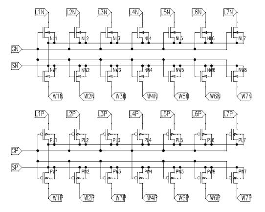
Fig 1 – Internal diagram of circuit
Details
of technology TSMC TSMC 00.335
1. Process
Description
MOSIS 0.35 micron multi-project runs support both processes using epitaxial
wafers. Stacked contacts/vias are supported by either process.
Both TSMC35_P2 and TSMC35_SIL require Metal 4 in the pad stack.
TSMC35_P2
TSMC35_P2 is the TSMC design technology for the double poly process (no
silicide block). It supports via3 and metal4, and is for 3.3 volt applications.
A thick oxide layer can be used for 5.0 volt transistors. 5 V ESD is available
as an option. PiP (poly2 over poly) capacitors (850 aF/µm²) are available.
Silicide block is not applicable to this polycided process.
TSMC35_SIL
TSMC35_SIL is the TSMC design technology for the single poly, silicided (with
silicide block for diffusion only) process. It supports 4 metal layers, and is
for 3.3 volt applications. A thick oxide layer can be used for 5.0 volt
transistors. 5 V ESD is available as an option.
2. Design Rules
These processes
support the following design rules
Note:
Stacked contacts/vias are supported by this process.
Review the following CMP
and antenna guidelines which apply
to both sets of design rules.
MOSIS
Technology Codes
See
Technology Codes and Layer Maps for TSMC 0.35 Micron
4
Metal, 2 Poly, Polycide Process
4
Metal, 1 Poly, Silicide Process
Important
note about insulator layers
On this
process, TSMC requires that all features on the insulator layers (CONTACT, VIA,
VIA2, VIA3) be of the single standard size. There are no exceptions for pads, logos,
or anything else. Large openings are to be replaced by an array of standard
sized openings.
A.
Process Description
MOSIS 0.35 micron multi-project runs support both processes using epitaxial
wafers. Stacked contacts/vias are supported by either process.
Both TSMC35_P2 and TSMC35_SIL require Metal 4 in the pad stack.
TSMC35_P2
TSMC35_P2 is the TSMC design technology for the double poly process (no
silicide block). It supports via3 and metal4, and is for 3.3 volt applications.
A thick oxide layer can be used for 5.0 volt transistors. 5 V ESD is available
as an option. PiP (poly2 over poly) capacitors (850 aF/µm²) are available.
Silicide block is not applicable to this polycided process.
TSMC35_SIL
TSMC35_SIL is the TSMC design technology for the single poly, silicided (with
silicide block for diffusion only) process. It supports 4 metal layers, and is
for 3.3 volt applications. A thick oxide layer can be used for 5.0 volt
transistors. 5 V ESD is available as an option.
B. Design Rules
These processes support the following design rules
Note: Stacked contacts/vias are supported by this
process.
Important note about insulator layers
On this process, TSMC requires that all features on
the insulator layers (CONTACT, VIA, VIA2, VIA3) be of the single standard size.
There are no exceptions for pads, logos, or anything else. Large openings are
to be replaced by an array of standard sized openings.
Description of the transistors
Considerations:
·Lambda (l): 0.25mm
·Smallest
channel length in our design: 2l = 0.5mm
·Smallest channel
width in our design: 2l = 0.5mm
·Technology
used: SCMOS
Lay Out
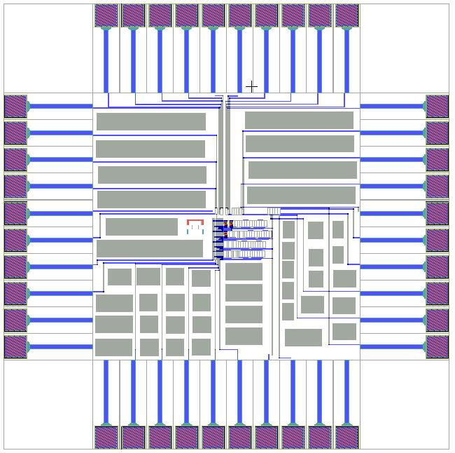
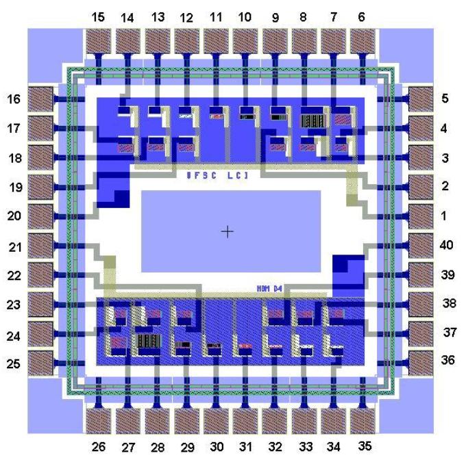
Fig 2 L– Lay Outayout
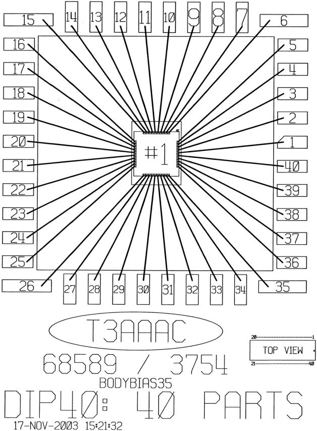
TSMC 0.3TSMC 0.35
Pin
Description
Description of the transistors
Considerations:
Lambda (l): 0.2mm
Smallest
channel length in our design: 2l = 0.4mm
Smallest
channel width in our design : 5l = 1mm
Technology
used: SCMOS_SUBM
References
[1] H. Soeleman,
K. Roy, “Ultra-Low Power Digital Subthreshold Logic Circuits”, International
Symposium on Low Power Electronics and Design, 1999, pp.94-96.
[2]
H. Soeleman, K. Roy, B. Paul, “Sub-Domino Logic: Ultra-Low Power Dynamic Sub-Threshold
Digital Logic”, IEEE International Conference on VLSI and Design, 2001,
pp211-214.
[3]
Amirtharajah, R., Chandrakasan, A., “Self-Powered Signal Processing Using
Vibration-Based Power Generation”, IEEE J. Solid-State Circuits, vol. 33, No.
5, May 1998.
[4] Bolcloni, L., Borgatti, M.,
Felici, M., Rambaldi, R., Guerrieri, R., “A
low-power, voice-controlled, H.263 video decoder for portable applications”,
IEEE Journal of Solid-State Circuits, vol. 33, no. 11, November 1998.
[5]
A. Bryant, J. Brown, P. Cottrell, M. Ketchen, J. Ellis-Monaghan, E. Nowak,
“Low-Power CMOS at Vdd=4kT/q”, Device Research Conference 2001.
Pads diagram