A Gm-C Bump Equalizer
For Low-Voltage Low-Power
Applications
Summary
Submitted by: Renato
Galembeck, renato@eel.ufsc.br Marcelo Luiz Poleto
poleto@eel.ufsc.br
Professor: Márcio Cherem Schneider, marcio@eel.ufsc.br
Affiliation: Integrated
Circuits Laboratory-Department of Electrical Engineering-Federal University of
Santa Catarina. (www.eel.ufsc.br/lci)
Project Title: A Gm-C Bump Equalizer For
Low-Voltage Low-Power Applications
Fabrication Technology:
TSMC 0.35
Chip size: 1.5mmx1.5mm
Packaging: DIP- 40.
Project Description
Graphic equalizers are filters aimed to change the amount of
equalization without altering the
shape of the transfer characteristic [1]. Particularly,
bump-equalizers [1] - [3] are applied in audio
systems to provide hearing-impaired people with improved
sound quality by equalization of the
frequency response. Implementations of bump-equalizers using
either MOSFET-C [1] or switchedcapacitor
techniques [2], [3] have already been reported.
This work focuses on the design of a parametric equalizer
intended for hearing-aid applications.
The 2nd-order low-voltage low-power (LVLP) continuous time
bump-equalizer comprises a
bandpass section and a programmable current amplifier. The
main building block is an OTA, who se
small-signal transconductance depends linearly on the
drain-to-source voltage of the input
MOSFET operating in the triode region [4], [5]. One of the
most appealing features of our filter is
that the building blocks, namely the programmable current
mirror, the Q-control block, and the
common-mode feedback circuit are derived from the basic
transconductor topology. Moreover, the
tuning strategy is very simple – an external DC voltage
directly tunes the bump-equalizer center
frequency fo, while two digital words control the Q-factor
and the bump/dip coefficient.
Fabrication Process
The design was submitted to TSMC 0.35mm process.
(TSMC35_P2). This process was
chosen because it is fully compatible with our proposal and
we already have experience in this
technology. The project is being designed with the MOSIS
Scalable CMOS (SCMOS) Design Rules,
SCNE.
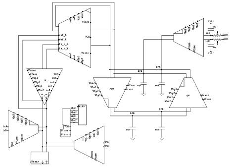
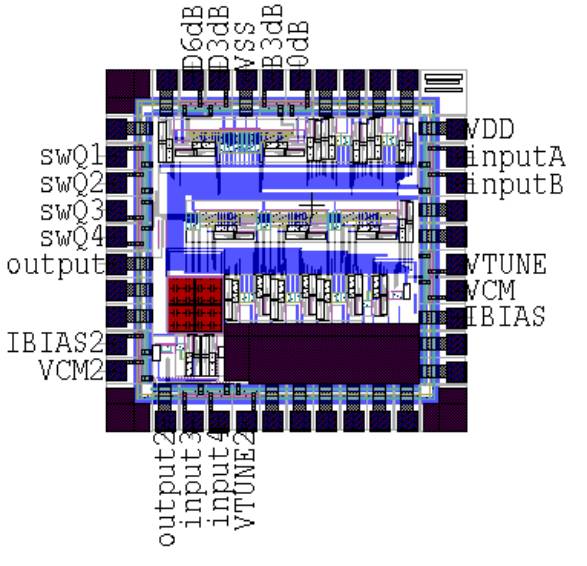
Estimated Structures and Chip Size
To validate the proposed structure a test structure was
designed. It is composed of one
isolated transconductor (figure 1) with its respective
common-mode feedback bias circuit (figure 2).
The bump equalizer (figure 3) will also be integrated. The
whole design fits in a 1.5mmx1.5mm die,
including pads. A conventional 40-pin (DIP40) package
supplied by MOSIS was used.
Layout
References
[1] S. Sakurai et al., “A MOSFET-C variable equalizer circuit with simple on-chip automatic tuning,”
IEEE JSSC, vol. 27, no. 6, pp.
927-934, June 1992.
[2] J. F. Duque-Carrillo, J. Silva-Martínez, and E.
Sánchez-Sinencio, “Programmable witched capacitor bump equalizer architecture,”
IEEE JSSC, vol. 25, no. 4, pp. 1035-1039, August 1990.
[3] J. F. Duque-Carrillo
et al. “VERDI: An acoustically programmable and adjustable CMOS mixedmode
signal processor for hearing aid applications,” IEEE JSSC, vol. 31, no.
5, pp. 634-645, May 1996.
[4] J. L. Pennock, “CMOS triode transconductor for
continuous-time active integrated filters,”
Electronics Letters, vol. 21, no. 18, pp.
817-818, 29th August 1985.
[5] J. A. de Lima and C. Dualibe, “A linearly-tunable CMOS
transconductor with improved commonmode
stability and its application to gm-C filters,” IEEE TCASII, vol.48,
no.7, pp. 649-660, july 2001.