A low-power 8 bits successive Approximation ADC using Binary
weighted capacitors
Summary
To: MOSIS
Submitted by: Edgar
Mauricio Camacho Galeano, maoedgar@eel.ufsc.br
Professor: Márcio Cherem Schneider,
marcio@eel.ufsc.br
Affiliation: Integrated
Circuits Laboratory-Department of Electrical Engineering-Federal University of
Santa Catarina. (www.eel.ufsc.br/lci)
Project Title: A
low-power 8 bits successive approximation ADC.
Fabrication Technology: TSMC-0.35m
Objective: Design of a low-power successive
approximation ADC for applications requiring precision of 8 bits.
Challenges: Power DC consumption of 100mW at 3.0 Volts of power supply voltage.
Expected Publications: Publish our
results in international conferences.
Simulation support: Smash circuit simulator, L-edit Tanner.
Chip size: 1.500mmx1.500mm @2.25mm2 (TSMC 0.35mm)
Test: Measurement
of DC characteristics (INL, DNL), Measurement of AC characteristics by FFT (SNR
and ENOB vs input signal frequency)
Equipment: TDS2014
tektronix, HP4145B, HP3245A, HP E3610A, HP 3588A.
Packaging: DIP-
40.
Overview
One of the most popular types of successive
approximation architectures in CMOS technology uses the binary-weighted
capacitor array as its DAC. Called a charge redistribution successive
approximation ADC. This converter samples the input signal and then performs
the binary search based on the amount of charge on each of the DAC capacitors.
A comparator control the direction of the binary search, and the output of the
successive approximation register (SAR) is the actual digital conversion. This
technique is adequate for achieve low power consumption and moderate resolution
in the processing of low frequency signals. Also, this technique achieves
resolution until 10 bits without require of additional trimming techniques. One
important advantage is its insensitivity to the bottom-plate parasitic of MOS
capacitors, because the bottom plate is all times switched between a buffered
voltage reference and ground.
One most sources of error during the process of conversion
are the capacitor mismatch and the offset voltage associated with the
comparator. However, offset cancellation techniques or low offset comparators
can largely eliminate this inconvenient. The capacitor mismatch error has a big
impact over the monotonic behavior of the ADC. Therefore, the smaller capacitor
(LSB-DAC) must be calculated according to the precision required.
Project Description
This project proposes an 8 bits successive approximation A/D converter dedicated to sensing applications, which is suitable for low power applications. The ADC analog part was designed to operate at 3.0 volts of power supply voltage with 30uA of current consumption. Additional on-chip current sources will be also integrated. The ADC designed has been simulated using SMASH with TSMC 0.35 BSIM3V3 model. Simulation results for clock frequency of 50Khz shown that, it ADC can achieve 8 bits of precision when considering 0.4% of capacitor mismatching error. The circuit will test in our laboratory, where all the equipment necessary is available. The total silicon area needed including pads and test circuits is estimated at 1.500mmx1.500mm.
To characterize our chip, we will use an HP 4145B parameter analyzer, an HP 3588A Spectrum analyzer and a Tektronix TDS2014 digital oscilloscope.
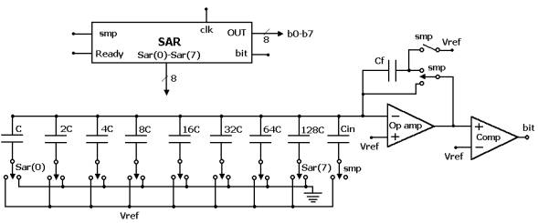
Figure 1. Schematic of the ADC
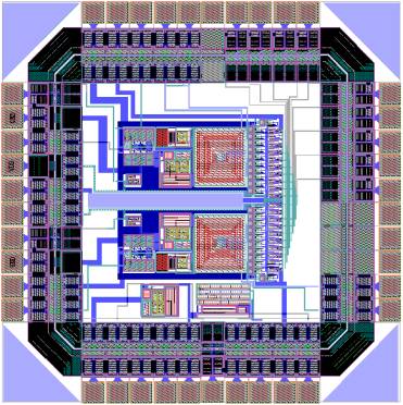
LAYOUT
References
[1] R. J.
Baker, H. W. Li, D. E. Boyce: CMOS Circuit Design, Layout and Simulation, IEEE
Press, 1st ed, 1998.
[2] D. Johns, K. Martins, Analog Integrated
Circuit Design, J. Wiley and Sons, 1st ed, 1996