NMOS and PMOS Transistor Arrays for Current
Mismatch Measurement
Summary
Submitted
by: Hamilton Klimach,
klimach@eel.ufsc.br
Professor: Márcio Cherem Schneider, marcio@eel.ufsc.br
Affiliation: Integrated Circuits Laboratory-Department
of Electrical Engineering-Federal University of Santa Catarina.
(www.eel.ufsc.br/lci)
Project
Title: Test Devices for
a Consistent Model for Drain Current Mismatch in MOSFETs
Fabrication Technology: AMI 1.5; AMI 0.5 and TSMC 0.35
Objective: having real measurements to support a new approach
for accurate MOS transistor matching calculation that is being developed, valid
for any operation region.
Challenges: establishing
a relationship among drain mismatch of identical MOS transistors and operation
region (inversion level, saturation condition and bulk bias).
Expected Publications: international conferences, journals and a PhD
Thesis.
Simulation support:
Smash circuit simulator, L-edit Tanner.
Chip size: 1.5mmx1.5mm
Test:
Measurement of DC characteristics.
Equipment: TDS2014 tektronix, HP4145, HP3245A, HP
E3610A, HP 3588A.
Packaging: DIP- 40.
Overview
It is widely
recognized that the performance of most analog or even digital circuits is
limited by MOS transistor matching [1-4]. The shrinkage of the dimensions of
MOSFETs and the reduction in the supply voltage make matching limitations even
more important to such an extent that several new studies have been published
in recent years [5-8]. Existing mismatch models use either simple drain current
models limited to a specific operating region [1, 2, 4, 7, 8] or complex
expressions [6] like that of BSIM. In general, however, the applicability of dc
current models to characterize mismatch is not questioned. It is widely
accepted that matching can be modeled by the random variations in geometric,
process and/or device parameters. The effect of the random parameters on the
drain current is quantified using the dc model of the transistor. As pointed
out in [7, 8] there is a fundamental flaw in this approach that results in
inconsistent modeling of matching. In effect, mismatch models implicitly assume
that the actual values of the lumped model parameters can be obtained
integrating the position-dependent distributed models over the areas of the
channel region of the device, e.g., for the threshold voltage VT
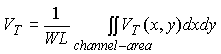 (1)
(1)
where W and L
are the width and the length of the transistor.
As analyzed
in [7, 8], the application of (1) to series or parallel association of
transistors leads to an inconsistent model of matching owing to the nonlinear
nature of MOSFETs. Consequently, the simple consideration of random
fluctuations in the lumped parameters of the dc current model is not appropriate
to develop matching models and new formulas must be derived from basic
principles.
Fortunately,
the formalism needed to model matching is already available in low frequency
(LF) noise modeling. In this new model, it is shown that the carrier number
fluctuation theory [9], employed to derive LF transistor noise, can be adapted
to model current matching in MOSFETs. To obtain general results for all bias
regions of the transistor we have used the Advanced Compact MOSFET (ACM) model,
a physics-based one-equation all-region model [10].
Project Description
A mismatch
test circuit was designed and fabricated in the AMIS 0.5mm 5V CMOS n-well process, through the MOSIS
Education Program (MEP). It is composed of a set of NMOS and PMOS transistors
disposed in arrays of 20 identical functional devices, surrounded by dummy ones
to ensure uniform boudary conditions for all active transistors, improving
matching properties. Transistor dimensions (WxL) of each array are 16.8mm x 11.2mm (large), 4.2mm x 2.8mm (medium), 1.05mm x 11.2mm (narrow - minimum width), 16.8mm x 0.7mm (short - minimum length) and 1.05mm x 0.7mm (small - minimum size), and they
are disposed side by side in rows. Wide metal conections and multiple contact
windows were designed to lower ohmic drops. Devices of each array have
identical design and current orientation. Fig. 1 shows a schematic diagram of
two arrays (one NMOS and the other PMOS)
of our test circuit. Five pairs of arrays composed by 20 NMOS and PMOS
transistors having the same dimensions are conected with drain, source and bulk
in parallel, being the selection made by individual gate terminals for each
array. Using this multiplexing strategy, it was possible to access 200
transistors in a 40 pin DIP package.
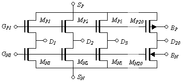
Schematic diagram of each
pair of arrays with the same dimensions.
Layout
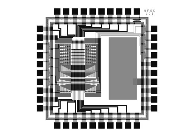
Circuit
layout. Transistor arrays for mismatch characterization are in the left part of
the die. Unused area was full-filled with metal and poly in agreement with
MOSIS instructions.
References
[1] J-B Shyu, G. C. Temes, and
F. Krummenacher, “Random error effects in matched MOS capacitors and current
sources”, IEEE J. Solid-State Circuits,
vol. 19, no. 6, pp. 948-955, Dec. 1984.
[2] M. J. M. Pelgrom, A. C. J.
Duinmaijer, and A. P. G. Welbers, “Matching properties of MOS transistors”, IEEE J. Solid-State Circuits, vol. 24,
no. 5, pp. 1433-1440, Oct. 1989.
[3] F. Forti and M. E. Wright,
“Measurements of MOS current mismatch in the weak inversion region”, IEEE J. Solid-State Circuits, vol. 29,
no. 2, pp. 138-142, Feb. 1994.
[4] M. J. Chen, J. S. Ho, and
T. H. Huang, “Dependence of current match on back-gate bias in weakly inverted
MOS transistor and its modeling”, IEEE J.
Solid-State Circuits, vol. 31, no. 2, pp. 259-262, Feb. 1996.
[5] J. A. Croon et al., “A
comparison of extraction techniques for threshold voltage mismatch”, Proc. IEEE 2002 Int. Conference on
Microelectronic Test Structures, pp. 235-240, 2002.
[6] P. G. Drennan, and C. C. McAndrew,
“Understanding MOSFET mismatch for analog design”, IEEE J. Solid-State Circuits, vol. 38, no. 3, pp. 450-456, March
2003.
[7] M-F. Lan and R. Geiger,
“Impact of model errors on predicting performance of matching-critical
circuits, 43rd. IEEE Midwest
Symp. on Circuits and Systems, pp.1324-1328, 2000.
[8] M-F. Lan and R. Geiger,
“Modeling of random channel parameter variations in MOS transistors”, IEEE International Symposium on Circuits and
Systems (ISCAS), vol. I, pp.85-88, 2001.
[9]
S.Cristensson, I.Lundstrom, C.Svensson, “Low
frequency noise in MOS transistors”, Solid-State Electron, vol.11, pp.797-812,
1968.
[10] A. I. A. Cunha, M. C.
Schneider, C. Galup-Montoro, “An MOS
transistor model for analog circuit design”, IEEE J Solid-State Circuits, vol.33, no.10, pp.1510-1519, Oct.1998.